
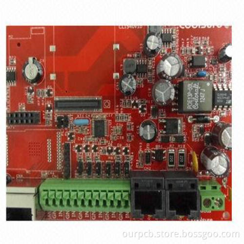

High density multilayer PCB board production factory
- Payment Type:
- T/T, PayPal or Western Union
Quantity:
Your message must be between 20 to 2000 characters
Contact NowBasic Info
Basic Info
| Payment Type: | T/T, PayPal or Western Union |
|---|
Product Description
Product Description
- -layer: 0.40mm
- 6-layer: 0.80mm
- 8-layer: 1.00mm
- 10-layer: 1.20mm


Related Keywords
Related Keywords


